
PCB design
The challenge of today’s PCB layout design is to accomplish for the increasing density of nets and components whilst reducing the PCB size area. Both electrical and mechanical requirements have to be fulfilled without affecting the overall electrical response, the PCB compliance, reliability and manufacturability. The ongoing trend of miniaturization is pushing the PCB design to a completely new level of complexity, that has to be overcome while satisfying the market demand of competitive prices and fast delivery. Investing in EDA softwares and technologies, together with fruitful and stimulating collaborations, is the key of our success.
We are proud of our proven experienced.
Each PCB design has unique needs, and guidelines must be customized as required. We work closely with clients to assess specific PCB layout challenges from low-cost commercial products to more complex concepts. Using our highly specialized custom PCB designers will get your innovative concepts to market fast. The PCB design team works seamlessly with customers providing a rapid design and prototyping service for any project no matter how intricate the design and layout are.
We understand that our customers require a PCB design service which is rapid, accurate, flexible and driven by quality.
The team at pcb design is a group of dedicated professionals who ensure that this level of service is reached and exceeded where they can. We use regular communication via telephone and email to keep you up to speed with the progress of your board. The design service we offer is as inclusive as possible to ensure that, even if a PCB designer is not onsite with you, you have access to the crucial information about the progress of the project.
Our PCB Design respecting standard IPC
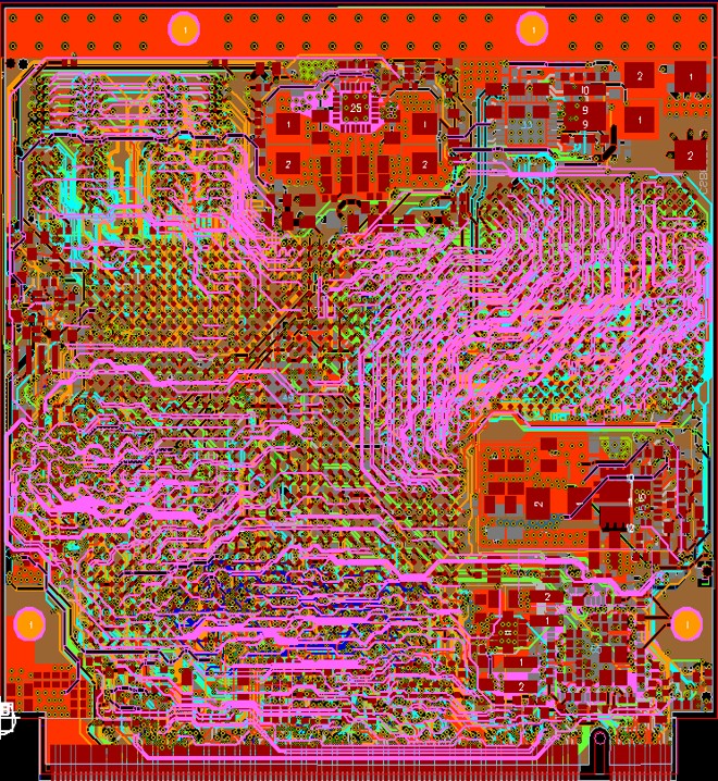
Technologies
Our designers are extremely well versed with today's technologies and their complex timing and topology requirements.
Digital Processor
Chip Sets (Intel and AMD) , Memory (DDR2, DDR3, and DDR4) and Interfaces (USB3.0, PCIe, SFP/SFP+, SATA, etc).
FPGA
Analog, Low level high sensitivity circuits, High power, Data acquisition
Power
High voltage,High current and Switchers
RF
Modems, Satellite communications and Radar
Mixed Technologies
All of the above Manufacturing HDI (micro, blind, and buried vias) ICT / Flying Probe Chip On Board (COB) and Rigid-Flex
PCB Documentation
ODB++
GERBER FILE SET
FABRICATION & ASSEMBLY DRAWINGS
PICKUP AND PLACE FILE
LAYOUT FILE
3D FILE
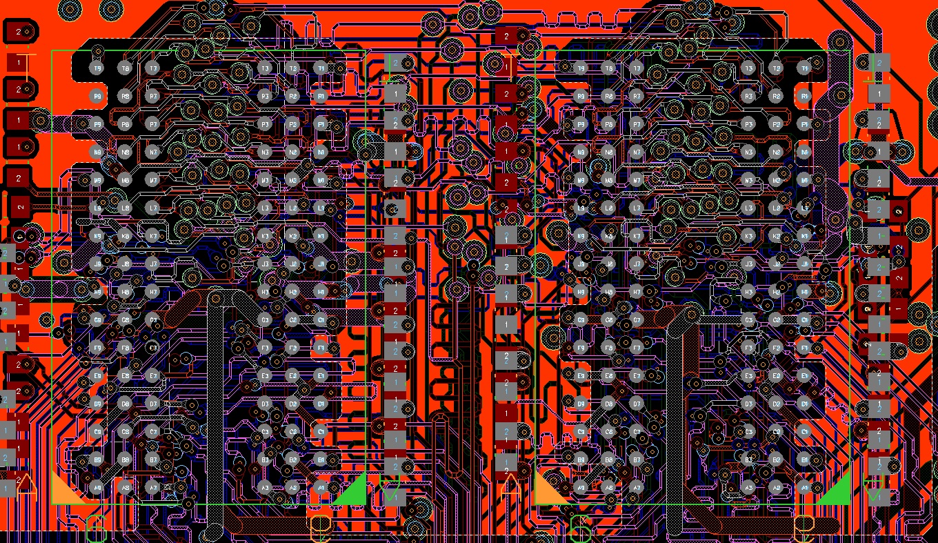
DDR3-1866